Create Your First Project
Start adding your projects to your portfolio. Click on "Manage Projects" to get started
FPGA SPI Master for 12Bit ADC interfacing
Project type
Embedded Systems
Date
June 2023
Location
San Diego, CA
Successfully got transfer rates of 500ksps with a 8MHZ clock frequency. Multiplexed design of the input data allowed me to source all 8-channels of the ADC for multi-axis applications.
Wrote custom System Verilog scripts to accurately parse SPI data from a TI ADC128S102. This involved utilizing a Xilinx Vivado environment to offload bitstreams to a Artix-7 FPGA.
For initial validation I made a simple testbench that tests the FPGA's ability to transmit data to the ADC (MOSI) as well as checking the SPI clock frequency. Later I moved to debugging the MISO data with an ILA core provided by Vivado as well as using Liquid Instruments Moku:Go for logic level analysis. Using the ILA core I was able to preform real-time waveform debugging ultimately allowing me to pinpoint problems in bit parsing, synchronization issues, and overall reliability.
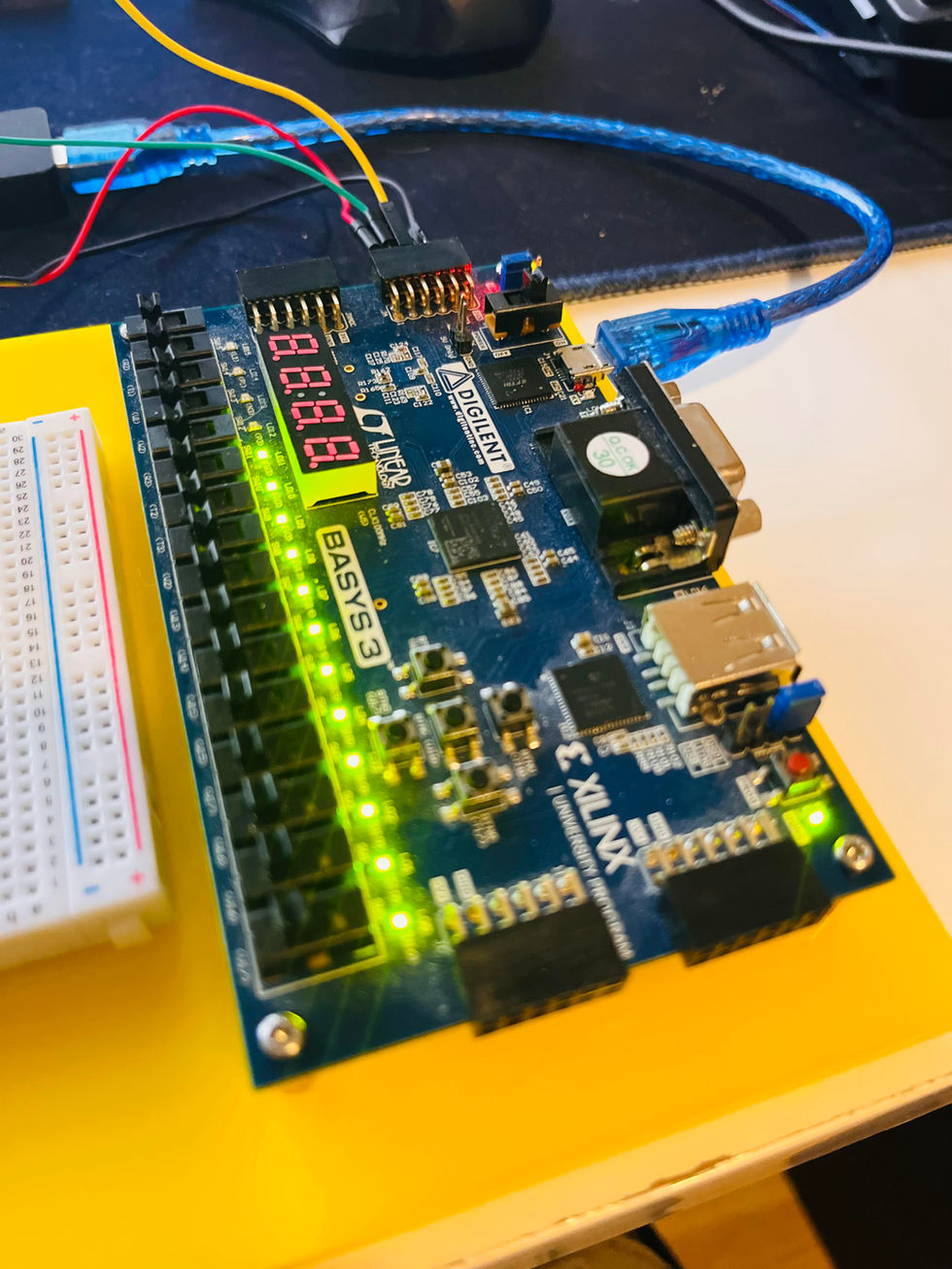
Side note: I created a test fixture out of 1/4" acrylic that housed the ADC eval. board, FPGA and a breadboard for interconnects between them.


